Nikon has announced a new digital lithography system for semiconductor backend processes, featuring 1.5μm resolution and 30% higher productivity than comparable tools, processing up to 65 substrates per hour.
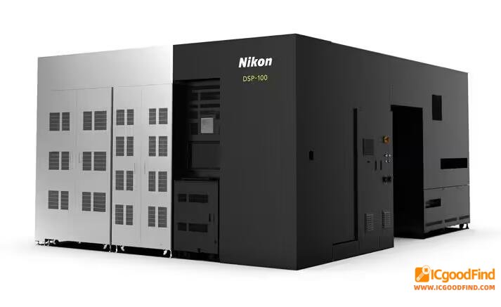
The company introduced its first backend patterning system, the DSP‑100 (1μm resolution, 50 panels per hour for 510×515mm substrates) in July 2025. The new machine shares the same platform as the DSP‑100 but targets different performance advantages, allowing flexible matching to diverse production needs.
As panel‑level packaging (PLP) becomes mainstream for backend processes, demand varies across large interposers and FC‑BGA substrates. By swapping optical components, the new tool can also achieve 1μm resolution , offering high flexibility.
ICgoodFind: Nikon’s latest backend steamer balances resolution and throughput on a common platform, broadening packaging lithography options.
