Intel TE28F800B3B110: A Deep Dive into the 8-Megabit Flash Memory Chip
In the landscape of late-1990s and early-2000s electronics, Intel’s flash memory solutions were pivotal in enabling a new generation of digital devices. Among these, the Intel TE28F800B3B110 stands out as a quintessential 8-megabit (1MB) chip that powered everything from networking equipment and set-top boxes to early BIOS firmware. This deep dive explores the architecture, functionality, and lasting impact of this foundational component.
Constructed using Intel's advanced 0.25-micron ETOX™ II process technology, the TE28F800B3B110 was a leader in performance and reliability for its time. Organized as 1,048,576 words of 8 bits each (8Mb), or configured in a 16-bit data bus mode for wider access, its versatility was a key strength. This chip belonged to the Intel Advanced+ Boot Block family, a feature set specifically designed for code and data storage in embedded systems. Its architecture divided the memory array into multiple blocks, with a small, protected boot block at the top or bottom of the address space. This was crucial for storing critical boot code, safeguarding it from accidental erasure or overwrite during main firmware updates.
The chip operated on a single 3.3-volt power supply, a significant advantage over older 5V parts, which translated to lower power consumption—a critical factor for portable and battery-powered devices. Its command set was compatible with the JEDEC common flash interface, simplifying integration for designers. Key operations—byte/word program, block erase, and read—were all executed through a write state machine, managed by on-chip intelligence that automated the complex timing and voltage algorithms required. This meant the host processor simply issued a command, and the chip handled the rest, significantly reducing the system's processing overhead.
A critical aspect of its design was robust data integrity. The chip supported a minimum of 100,000 program/erase cycles per block, ensuring longevity in applications requiring frequent firmware writes. Furthermore, it offered multiple data protection mechanisms, including hardware-based write protection via the `WP` pin and a software locking feature for individual blocks, preventing unauthorized modifications.
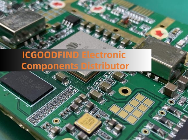
In application, the TE28F800B3B110 was often found soldered onto motherboards or embedded into specialized controller cards. It served as the non-volatile storage heart, holding the initial system boot instructions before the main operating system could take over. Its reliability and performance made it a trusted choice in an era where firmware stability was paramount.
ICGOODFIND: The Intel TE28F800B3B110 is a classic example of a highly optimized, application-specific memory solution. Its legacy lies in its balanced architecture, which successfully merged performance, density, and robust security features for the embedded market. It exemplifies the transition towards lower-voltage, higher-reliability flash memory that became the standard for decades to follow.
Keywords: Intel Flash Memory, Boot Block Architecture, 3.3V Operation, ETOX™ Process, Non-volatile Storage